
As the calendar turns to 2026, the semiconductor industry is standing on the precipice of its most significant architectural shift in decades. The traditional organic substrates that have supported the world’s microchips for over twenty years have finally hit a physical wall, unable to handle the extreme heat and massive interconnect demands of the generative AI era. Leading this charge is Intel (NASDAQ: INTC), which has successfully moved its glass substrate technology from the research lab to the manufacturing floor, marking a pivotal moment in the quest to pack one trillion transistors onto a single package by 2030.
The transition to glass is not merely a material swap; it is a fundamental reimagining of how chips are built and cooled. With the massive compute requirements of next-generation Large Language Models (LLMs) pushing hardware to its limits, the industry’s pivot toward glass represents a "break-the-glass" moment for Moore’s Law. By replacing organic resins with high-purity glass, manufacturers are unlocking levels of precision and thermal resilience that were previously thought impossible, effectively clearing the path for the next decade of AI scaling.
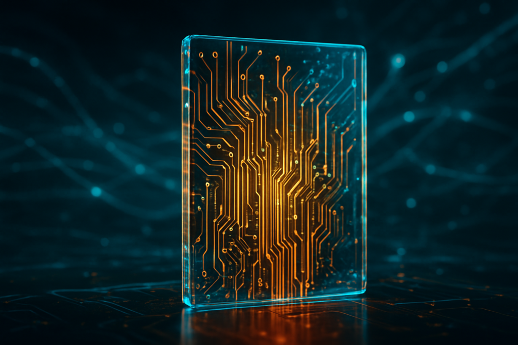
The Technical Leap: Why Glass is the Future of Silicon
At the heart of this revolution is the move away from organic materials like Ajinomoto Build-up Film (ABF), which suffer from significant warpage and shrinkage when exposed to the high temperatures required for advanced packaging. Intel’s glass substrates offer a 50% improvement in pattern distortion and superior flatness, allowing for much tighter "depth of focus" during lithography. This precision is critical for the 2026-era 18A and 14A process nodes, where even a microscopic misalignment can render a chip useless.
Technically, the most staggering specification is the 10x increase in interconnect density. Intel utilizes Through-Glass Vias (TGVs)—microscopic vertical pathways—with pitches far tighter than those achievable in organic materials. This enables a massive surge in the number of chiplets that can communicate within a single package, facilitating the ultra-fast data transfer rates required for AI training. Furthermore, glass possesses a "tunable" Coefficient of Thermal Expansion (CTE) that can be matched almost perfectly to the silicon die itself. This means that as the chip heats up during intense workloads, the substrate and the silicon expand at the same rate, preventing the mechanical stress and "warpage" that plagues current high-end AI accelerators.
Initial reactions from the AI research community have been overwhelmingly positive, with experts noting that glass substrates solve the "packaging bottleneck" that threatened to stall the progress of GPU and NPU development. Unlike organic substrates, which begin to deform at temperatures above 250°C, glass remains stable at much higher ranges, allowing engineers to push power envelopes further than ever before. This thermal headroom is essential for the 1,000-watt-plus TDPs (Thermal Design Power) now becoming common in enterprise AI hardware.
A New Competitive Battlefield: Intel, Samsung, and the Packaging Wars
The move to glass has ignited a fierce competition among the world’s leading foundries. While Intel (NASDAQ: INTC) pioneered the research, it is no longer alone. Samsung (KRX: 005930) has aggressively fast-tracked its "dream substrate" program, completing a pilot line in Sejong, South Korea, and poaching veteran packaging talent to bridge the gap. Samsung is currently positioning its glass solutions for the 2027 mobile and server markets, aiming to integrate them into its next-generation Exynos and AI chipsets.
Meanwhile, Taiwan Semiconductor Manufacturing Co. (NYSE: TSM) has shifted its focus toward Chip-on-Panel-on-Substrate (CoPoS) technology. By leveraging glass in a panel-level format, TSMC aims to alleviate the supply chain constraints that have historically hampered its CoWoS (Chip-on-Wafer-on-Substrate) production. As of early 2026, TSMC is already sampling glass-based solutions for major clients like NVIDIA (NASDAQ: NVDA), ensuring that the dominant player in AI chips remains at the cutting edge of packaging technology.
The competitive landscape is further complicated by the arrival of Absolics, a subsidiary of SKC (KRX: 011790). Having completed a massive $600 million production facility in Georgia, USA, Absolics has become the first merchant supplier to ship commercial-grade glass substrates to US-based tech giants, reportedly including Amazon (NASDAQ: AMZN) and AMD (NASDAQ: AMD). This creates a strategic advantage for companies that do not own their own foundries but require the performance benefits of glass to compete with Intel’s vertically integrated offerings.
Extending Moore’s Law in the AI Era
The broader significance of the glass substrate shift cannot be overstated. For years, skeptics have predicted the end of Moore’s Law as the physical limits of transistor shrinking were reached. Glass substrates provide a "system-level" extension of this law. By allowing for larger package sizes—exceeding 120mm by 120mm—glass enables the creation of "System-on-Package" designs that can house dozens of chiplets, effectively creating a supercomputer on a single substrate.
This development is a direct response to the "AI Power Crisis." Because glass allows for the direct embedding of passive components like inductors and capacitors, and facilitates the integration of optical interconnects, it significantly reduces power delivery losses. In a world where AI data centers are consuming an ever-growing share of the global power grid, the efficiency gains provided by glass are a critical environmental and economic necessity.
Compared to previous milestones, such as the introduction of FinFET transistors or Extreme Ultraviolet (EUV) lithography, the shift to glass is unique because it focuses on the "envelope" of the chip rather than just the circuitry inside. It represents a transition from "More Moore" (scaling transistors) to "More than Moore" (scaling the package). This holistic approach is what will allow the industry to reach the 1-trillion transistor milestone, a feat that would be physically impossible using 2024-era organic packaging technologies.
The Horizon: Integrated Optics and the Path to 2030
Looking ahead, the next two to three years will see the first high-volume consumer applications of glass substrates. While the initial rollout in 2026 is focused on high-end AI servers and supercomputers, the technology is expected to trickle down to high-end workstations and gaming PCs by 2028. One of the most anticipated near-term developments is the "Optical I/O" revolution. Because glass is transparent and thermally stable, it is the perfect medium for integrated silicon photonics, allowing data to be moved via light rather than electricity directly from the chip package.
However, challenges remain. The industry must still perfect the high-volume manufacturing of Through-Glass Vias without compromising structural integrity, and the supply chain for high-purity glass panels must be scaled to meet global demand. Experts predict that the next major breakthrough will be the transition to even larger panel sizes, moving from 300mm formats to 600mm panels, which would drastically reduce the cost of glass packaging and make it viable for mid-range consumer electronics.
Conclusion: A Clear Vision for the Future of Computing
The move toward glass substrates marks the beginning of a new epoch in semiconductor manufacturing. Intel’s early leadership has forced a rapid evolution across the entire ecosystem, bringing competitors like Samsung and TSMC into a high-stakes race that benefits the entire AI industry. By solving the thermal and density limitations of organic materials, glass has effectively removed the ceiling that was hovering over AI hardware development.
As we move further into 2026, the success of these first commercial glass-packaged chips will be the metric by which the next generation of computing is judged. The significance of this development in AI history is profound; it is the physical foundation upon which the next decade of artificial intelligence will be built. For investors and tech enthusiasts alike, the coming months will be a critical period to watch as Intel and its rivals move from pilot lines to the massive scale required to power the world’s AI ambitions.
This content is intended for informational purposes only and represents analysis of current AI developments.
TokenRing AI delivers enterprise-grade solutions for multi-agent AI workflow orchestration, AI-powered development tools, and seamless remote collaboration platforms.
For more information, visit https://www.tokenring.ai/.